Manufacturing of printed circuit boards (PCB) with an automated surface mount assembly (SMA) line consists of the following sequence of operations:
- Solder paste application
- Component placement
- Reflow soldering
- Cleaning
- Electrical test
In order to achieve the optimal product throughput while at the same time ensuring minimal machine downtime, the operations need to be carefully planned and scheduled.
Production planning
With an increase in product variance across a number of different SMT production lines, it is critical to get an efficient production plan that can balance the production lines and optimize production performance.
Good solid design data is the first step. It includes PCB design data, full bill of materials (BoM), product references, placement data and net lists to allow for testing.
The SMT manufacturing process is BoM (bill of materials) driven, so a fully optimized component list is essential within the planning and scheduling steps.
Once all these data have been compiled and verified, the next step towards achieving an optimal production plan and schedule is to ensure the PCB can be produced with zero design errors (failure modes that are associated with poor design). This is done by completing a DFM analysis which ensures the following results:
- The design will yield good soldered joints;
- All parts can be placed in the intended positions;
- The actual PCB can be produced within the physical constraints of the manufacturing line capabilities.
An example of this would be the CAD design calls for a specific component to be placed on the board in a particular location. The CAD design shows solder pad sizes and locations that would match the ‘standard’ component listed, however, the component being purchased (correct device but from an alternative supplier) has a slightly different footprint and does not sit as intended. This could result in a product fault.
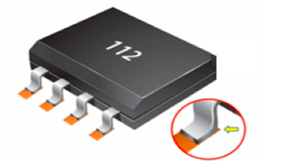
Figure: incorrect footprint on the solder pads
Once all this has been completed, a production data set can be compiled and generated. This would include Stencil design, machine programs for SMT, as well as through-hole technology (THT) parts, all inspection points as well as testing sequences.
From a planning and scheduling process aspect, work orders need to be loaded into a system that then combines all the data in order to generate the best product schedule in conjunction with production line availability.
Other aspects to take into consideration while planning for optimization
We talked about the process being BoM driven and it is the components on the BoM that become the critical factor when it comes to functionality of the printed circuit board.
It is paramount that the correct components are used and one major step in the overall process is inspection of incoming components. This will be the subject of a follow-on article.